AE-252 Week-5: MID-TERM EXAMClick schematic for the necessary reference material for the mid-term exam.
You can review the exam below or download the pdf document
good luck!
eddie
AE-252 Mid-term examNAME:_______________________________________ DATE:___________
The questions in this exam relate specifically to the power supply schematic for the Vari-fi JFET preamp kit, which can be downloaded at:
http://www.tangible-technology.com/ipr/AE230/html/wk_4/vari-fi/jfet_pre/VF_psu.html
PLEASE do the work in pencil, show all work (starting with formulae) and be sure to specify quantity (volts, amps, watts, dB, etc.).
- The Vari-fi JFET mic preamplifier consists of two gain stages each on its own printed circuit board (PCB). Each PCB requires 24-volts dc @ 40mA from the power supply unit (PSU). The equivalent resistance of each preamp board is _______________-ohms and each dissipates __________________ watts.
_______________________________________________________________
- The low-voltage secondary of the power transformer (xfrmr) connects to the PSU via connector ______________. The secondary has two ____-volt windings that have a common connection at J-1 pins ____ and ____. This common connection becomes _______________ and travels, from left to right, to pin-____ of J-2.
- Power for the preamps starts at the transformer secondary and is rectified by diodes _____ and _____, a __________-wave rectifier, after which the raw DC is filtered by __________.
- This is followed by a voltage divider that consists of _______ and ________ .
- The voltage drop across R-1 is____________________________________
_______________________________________________________________
- The current through R-1 is _______________________________________
_______________________________________________________________
- The power dissipated by R-1 is ___________________________________
________________________________________________________________
_______________________________________________________________
- The purpose of Z-1 is __________________________________________ .
- The base-emitter voltage drop for Q-1 should be _____________________.
- The measured base-emitter voltage is ______________________________.
- The preamp PCBs require approximately 24-volts and the PSU delivers within ______ per cent.
_______________________________________________________________
- As mentioned in question-1, when testing the PSU, two resistors simulated the load of each preamp module. These resistors were connected between J2 pin-3 and __________ (J-____ , pin-_____). In the schematic, the power supply output voltage is slightly higher and the closest standard resistor values (that were near at hand) were 620-? @ 1 watt each. What is the current through each resistor and the power dissipation?
________________________________________________________________
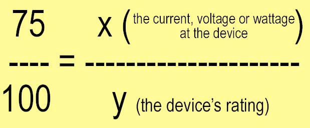
- For all device ratings - fuses (current), Resistors (wattage), Capacitors (voltage) - here is the formula to correlate the safe operating range so that it is within 75% of the devices rated value.
For example, a 20amp circuit breaker should see no more than 15 amps of continuous current. By using the formula and cross-multiplying (100x = 75*y = 100x = 75*20) you can see that (x = .75 * 20A = 15A) or x = 1500/100 = 15A. Conversely, if you know the current, voltage or wattage at the device, you can then calculate the safe rating above which the device should be rated.Based on this formula, calculate the safe power rating for the resistors in question-12 to the nearest rounded-up wattage (typical wattage values are 1/4, 1/2, 1, 2, 3, 5, 10).
______________________________________________________________________________________________________________________________
- The phantom power supply is fed from one leg of the xfrmr secondary through ______ and ______ before reaching the rectifier, which consists of ________ and _______. This circuit is essentially two ______-wave rectifiers in a _____________ _____________ configuration, named because it produces twice as much DC voltage than the RMS AC voltage feeding it.
- Once rectified, the raw DC is filtered by ________ and clamped at approximately _______ volts by the two series _____________, designated _____ and _____.
- The phantom power output appears at pin-_____ of J-_____
________________________________________________________________
________________________________________________________________
- The phantom power supply also fed a 3k4 resistive load to simulate the worst case scenario (shorting the the two ____-? phantom resistors at pin-2 and pin-3 of the XLR to ground).
- As stated in note-3 on the schematic, the no-load to worst case full-load output of the power supply ranges from 51.3 volts to 45.6 volts. This change in load is reflected back at R4. What is the AC current through, and the power dissipated by R4 from no-load to full-load?
_______________________________________________________________
_______________________________________________________________
- Is the wattage dissipated by R4 within 75% of the resistor's rating on the schematic? (show work)
_______________________________________________________________
- The power indicating LED is designated _____. Is it before or after the voltage regulator? ______________________________________________
_______________________________________________________________
- The resistor, R- _______, feeding the LED has to "throw away" _____ volts (VR3)in order to not blow up the LED. What is the current through R-4 and DL-1?
____________________________________________________________
_______________________________________________________________
- Based on all the information available to you, what is the voltage at DL-1?
