- Scott's ORIGINAL JFET article
- Protein Enriched JFET article (NEW 29 May 2013)
- Comparison of Scott's JFET schematic and our VF-13 Rev-2 schematic
- VariFi VF-13 Rev-2 Channel-1 (The schematic we will learn and draw)
- JFET Lab
- JFET Exercise
AE-237: Week-6
updated 17th September 2012
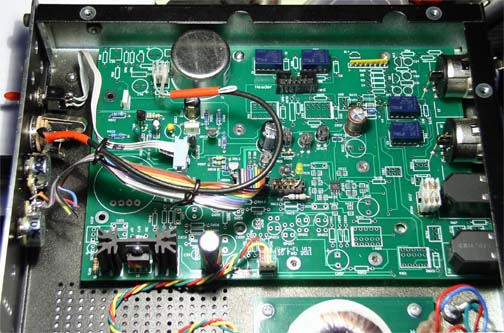
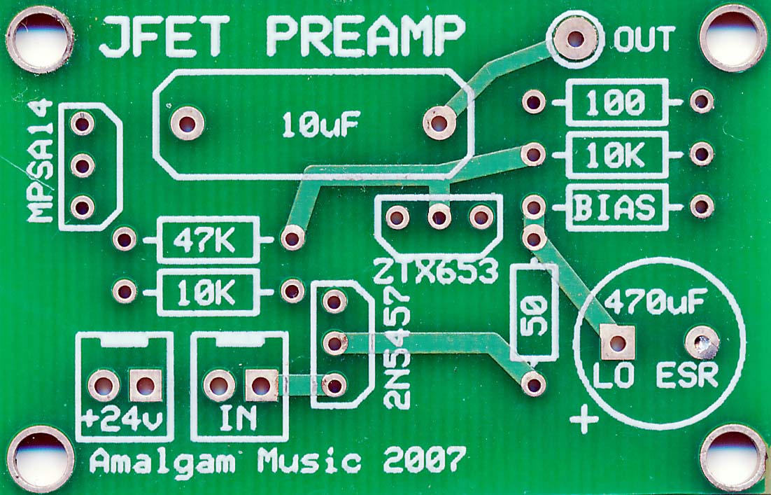
Our JFET Preamp was originally based on a circuit used by Scott Hampton in his HAMPTONE JFET preamps.
HOMEWORK: Read Scott's
Article and draw the simple JFET 15 times
HISTORY
|
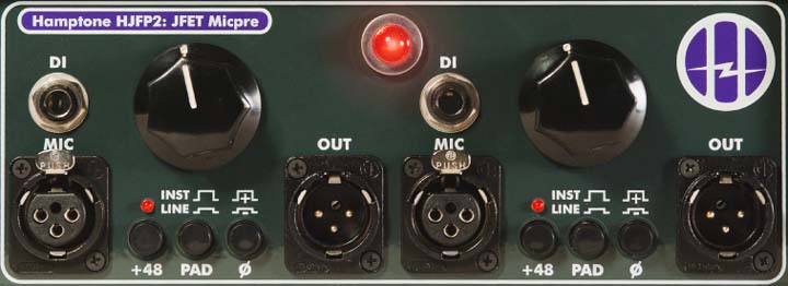 |
Circa 2007 |
 |
|
 |
- Circa 2010 ~ 2011
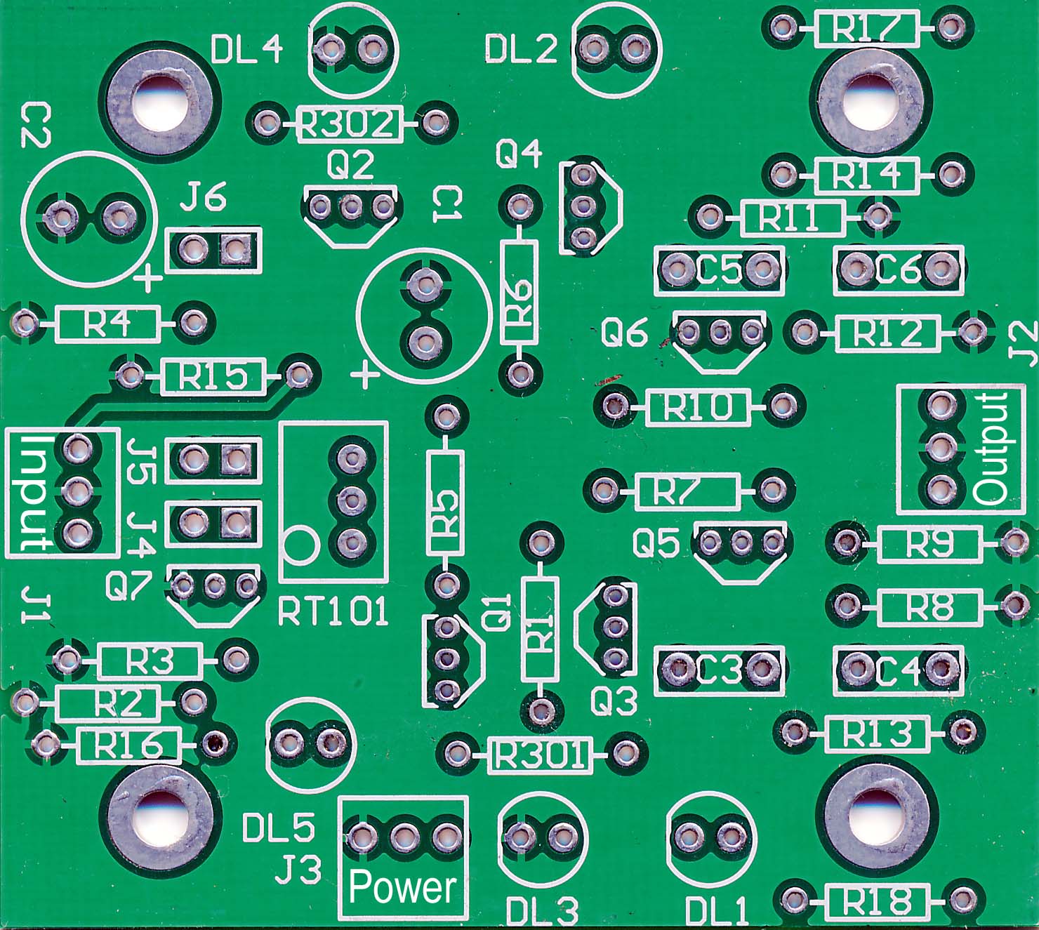
- After many experiements, the 'pastel' version of the circuit was finalized and committed to a full-sized PCB.
- The NEW circuit board - designated Vari-fi 13 - both layout and schematic, has become rather complex because it includes local 48v phantom and 30v regulation, PLUS an optional second channel and loop-thru buffer amp.
- Revision-2 of the PCB is finalized and replicated! The changes are mostly centered around fixing the ONE mistake on the first PCB, adding a bypass circuit to resolve a minor LF oscialltion issue and reconfiguring the headers to accomodate the new PCB layout.
- Right Angle Pot PCB design is complete. Schematic and PCB layout uploaded.
Circa 2012
we are using that details how the gain and limit pots are connected
March 2013:
as of 17th September 2012
|
|
|
|
|
|
|
|
|
|
|
|
|
|
|
|
|
|
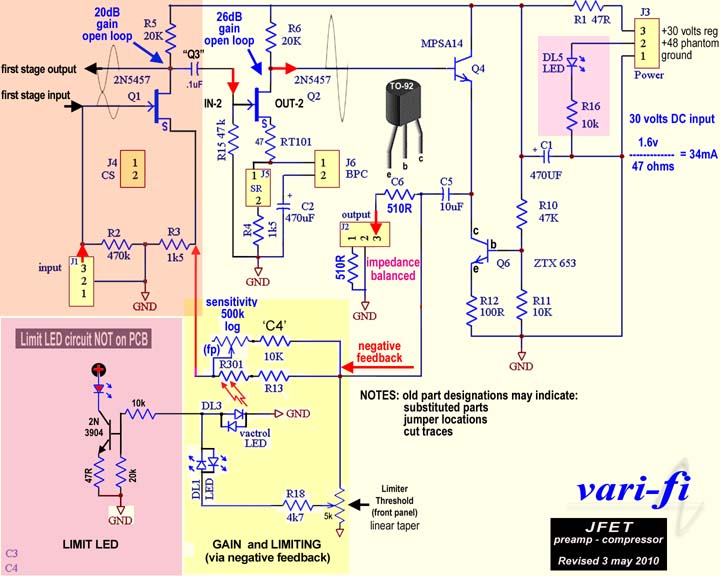
- Vari-fi DI: revised Spring 2010 (circuit with variable feedback and optical limiter)
- Please note that the yellow area of the circuit is identical to Scott's original / simple JFET circuit.
|
|
|
|
|
|
||
|
|
'instrument preamp' |
|
|
JFET schematic - Rev B |
|
|
|
|
|
|
* Note to self: Schematics and PCB have not yet been updated to REV B version (as of 14 March 2011)
Prototype in progress. The circuit is a morph of Scott Hampton's JFET and the Pultec MB-1 (vacuum tube). It can be mono or stereo. Mono version has a buffered loop through so Instruments taken direct can drive pedals and amps without affecting tone. Both mono and Stereo versions have optical limiting. Need to finish this mono version and build a stereo version to confirm that there are no mistakes, which so far I've only found one! Then, I need to design a front panel PCB and redesign the front panel.
